
RAM 2500 Truck 2WD L6-5.9L DSL Turbo VIN 7 (2001)
wire and 0 volts on the other bus wire.
The voltage drop through the termination resistor creates 2.51 volts on Bus (-), and 2.49 volts on Bus (+). The voltage difference between the two
circuits is 0.02 volts. When the data bus voltage differential is a steady 0.02 volts, the CCD system is considered "idle." When no input is received
from any module and the ignition switch is in the OFF position for a pre-programmed length of time, the bus data becomes inactive or enters the
"sleep mode." Electronic control modules that provide bus bias can be programmed to "wake up" the data bus and become active upon receiving
any predetermined input or when the ignition switch is turned to the ON position.
Bus Messaging
The electronic control modules used in the CCD data bus system contain microprocessors. Digital signals are the means by which microprocessors
operate internally and communicate messages to other microprocessors. Digital signals are limited to two states, voltage high or voltage low,
corresponding to either a one or a zero. Unlike conventional binary code, the COD data bus systems translate a small voltage difference as a one
(1), and a larger voltage difference as a zero (0). The use of the 0 and 1 is referred to as binary coding. Each binary number is called a bit, and
eight bits make up a byte. For example: 01011101 represents a message. The controllers in the multiplex system are able to send thousands of
these bytes strung together to communicate a variety of messages. Through the use of binary data transmission, all electronic control modules on
the data bus can communicate with each other.
The microprocessors in the COD data bus system translate the binary messages into Hexadecimal Code (or Hex Code). Hex code is the means by
which microprocessors communicate and interpret messages. When fault codes are received by the DRB III scan tool, they are translated into text
for display on the DRB III screen. Although not displayed by the DRB III for Body Systems, hex codes are shown by the DRB III for Engine
System faults.
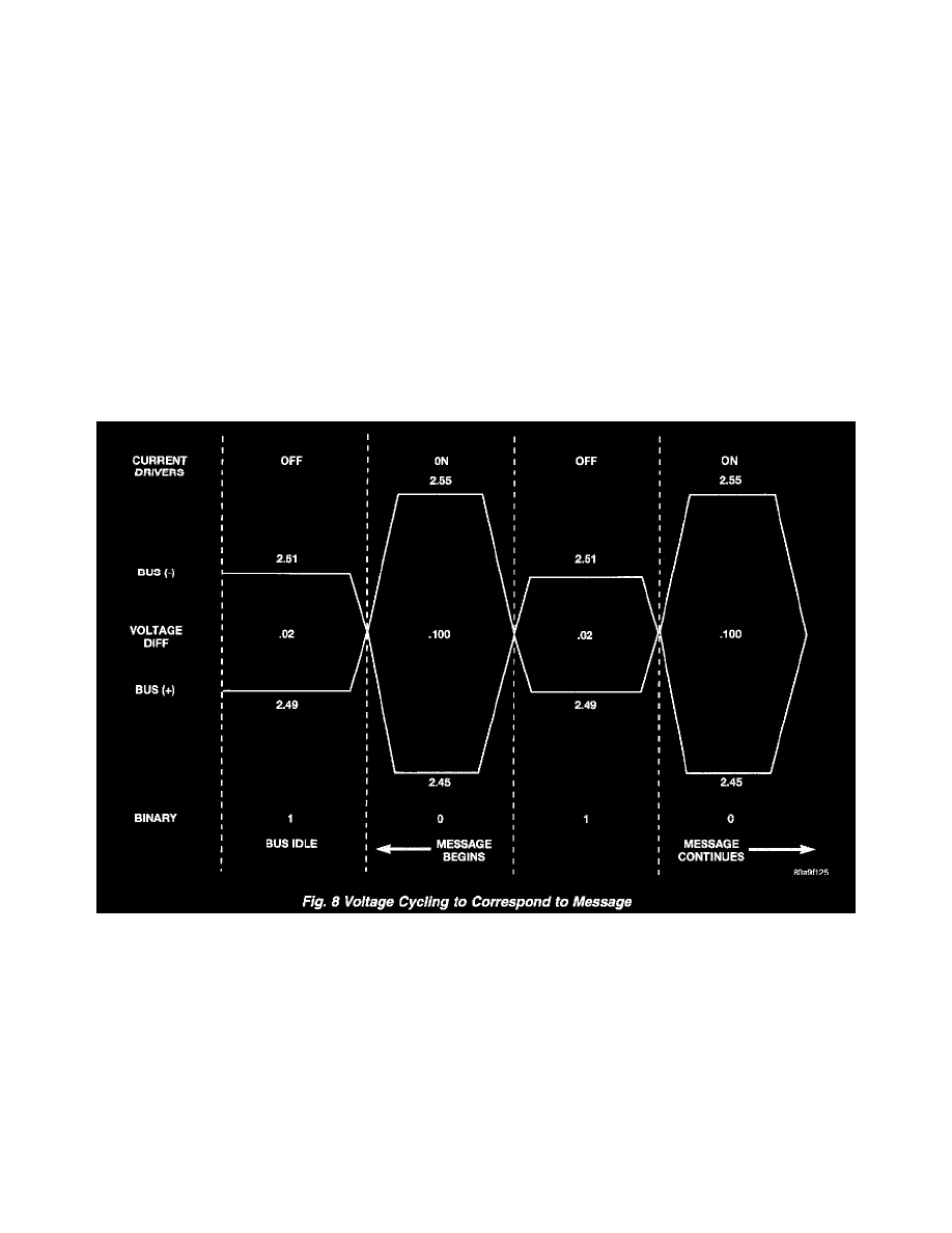
Fig.8 Voltage Cycling To Correspond To Message
When the microprocessor signals the transceiver in the CCD chip to broadcast a message, the transceiver turns the current drivers ON and OFF,
which cycles the voltage on the CCD data bus circuits to correspond to the message. At idle, the CCD system recognizes the 0.02 voltage
differential as a binary bit 1. When the current drivers are actuated, the voltage differential from idle must increase by 0.02 volt for the CCD
system to recognize a binary bit 0. The nominal voltage differential for a 0 bit is 0.100 volts. However, data bus voltage differentials can range
anywhere between 0.02 and 0.120 volt.
Bus Message Coding
The first part of a data bus message has an Identification (ID) byte. The ID byte contains message priority, message identification, message content
and message length information. All messages sent over the data bus are coded for both priority and identification.
Priority
Messages can be broadcast almost simultaneously by modules over the CCD data bus. Therefore, all messages are defined and ranked by a
predetermined priority. When two CCD chips start a message at exactly the same time, non-destructive arbitration occurs between the two CCD