
Grand Cherokee 4WD Laredo V8-4.7L (2002)
Data exchange between modules is achieved by serial transmission of encoded data over a single wire broadcast network. The PCI data bus
messages are carried over the bus in the form of Variable Pulse Width Modulated (VPWM) signals. The PCI data bus speed is an average 10.8
Kilo-bits per second (Kbps). Since there is only voltage present when the modules transmit and the message length is only about 500
milliseconds, it is ineffective to try and measure the bus activity with a conventional voltmeter. The preferred method is to use DRB III lab scope.
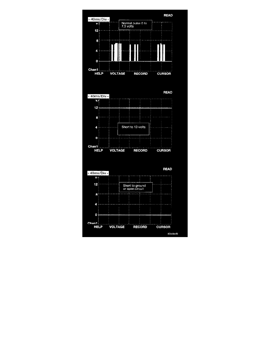
The 12v square wave selection on the 20-volt scale provides a good view of the bus activity. Voltage on the bus should pulse between 0 volts and
about 7-1/2 volts. Refer to the figure for some typical displays.
The voltage network used to transmit and receive messages requires biasing and termination. Each module on the PCI data bus system provides its
own biasing and termination. Each module (also referred to as a node) terminates the bus through a terminating resistor and a terminating
capacitor. The bus voltage is at 0 volts when no modules are transmitting and is pulled up to about 7-1/2 volts when modules are transmitting. The
Powertrain Control Module (PCM) is the only dominant node for the PCI data bus system.
The PCI bus uses low and high voltage levels to generate signals. The voltage on the bus varies between 0 and 7-1/2 volts. The low and high
voltage levels are generated by means of variable-pulse width modulation to form signals of varying length.
When a module is transmitting on the bus, it is reading the bus at the same time to ensure message integrity.
Each module is capable of transmitting and receiving data simultaneously.